Field Programmable Gate Array :A Process From Design to Deployment Demystified
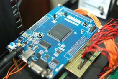 |
| Field Programmable Gate Array |
Field Programmable Gate Array (FPGAs) have emerged as a critical
component in the world of digital design and deployment. With their unique
ability to be customized and reprogrammed after manufacturing, FPGAs offer a
flexible and powerful solution for a wide range of applications.
The journey begins with the design
phase. Field
Programmable Gate Array designs typically start with a hardware
description language (HDL) such as VHDL or Verilog. Designers use these
languages to describe the desired behavior and functionality of the circuit.
They can create complex digital systems by interconnecting various logic
elements, such as gates, flip-flops, and arithmetic units, within the FPGA
fabric.
Once the design is complete, the
next step is synthesis. During this stage, specialized software tools convert
the high-level description into a netlist, which represents the logical structure
of the design. The netlist consists of interconnected logical components and
their interconnections.
After synthesis, the design
undergoes a process called place and route. This step involves mapping the
logical components onto specific physical resources within the Field Programmable Gate Array. The
software tool determines the optimal placement of components, taking into
account factors such as routing congestion and timing requirements. It then
determines the routing paths between the components to ensure proper
connectivity.
With the place and route complete,
the design enters the configuration phase. FPGAs are configured using a
bitstream—a binary file that contains the configuration information for the
FPGA fabric. The bitstream specifies the interconnections, logic functions, and
memory contents of the design. It is generated by the software tool and loaded
onto the FPGA device.
Once the Field Programmable Gate Array is configured, it is ready for
deployment. The deployed FPGA can perform a wide range of tasks, depending on
the specific design. FPGAs find applications in various domains, including
telecommunications, signal processing, robotics, aerospace, and many others.
Their flexibility allows for rapid prototyping, algorithm acceleration, and
even reconfigurable computing platforms.
One of the key advantages of FPGAs
is their ability to be reprogrammed. If changes or updates are required in the
design, the FPGA can be reconfigured with a new bitstream, eliminating the need
for costly hardware redesigns. This feature makes FPGAs highly desirable for
applications where flexibility, adaptability, and quick iterations are crucial.
A sensor is a device that
recognizes several kinds of physical input, including pressure, motion,
moisture, and light. To be processed further, this data is transmitted to an
electronic device. Sensors
are used by numerous industries, including electronics, IT &
telecommunications, automotive, and healthcare.
In conclusion, the journey of an Field Programmable Gate Array from design to deployment involves several stages and processes. Starting with the design phase, where the desired behavior is described using hardware description languages, followed by synthesis, place and route, and configuration. Once configured, FPGAs can be deployed for various applications, leveraging their flexibility and reprogrammability. The ability to modify the design without hardware changes makes FPGAs an attractive solution for prototyping and evolving digital systems. As technology continues to advance, FPGAs are expected to play an increasingly significant role in shaping the future of digital design and deployment.
Read more https://www.coherentmarketinsights.com/press-release/field-programmable-gate-array-market-4512


Comments
Post a Comment